A microcontroller is a compact integrated circuit designed to govern a specific operation in an embedded system. A typical microcontroller includes a processor, memory and input/output (I/O) peripherals on a single chip.
Sometimes referred to as an embedded controller or microcontroller unit (MCU), microcontrollers are found in vehicles, robots, office machines, medical devices, mobile radio transceivers, vending machines and home appliances, among other devices. They are essentially simple miniature personal computers (PCs) designed to control small features of a larger component, without a complex front-end operating system (OS).
- It is semiconductor device
- Consists of various Logic Circuits
- It is manufactured by using LSI or VLSI techniques
- Logic Circuits:
- Combinational Circuits: Gates, MUX
- Sequential Circuits: F/F, Memory
- Scale of Integration:
- SSI for less than 100 gates
- MSI for less than 1000 gates
- LSI for less than 1,00,000 gates
- SLSI for more than 1,00,000 gates
Memory of a microcontroller (or mostly any electronic device) is a physically built semiconductor capable of storing information in the form of bits (0s and 1s).
0s and 1s are actually voltage levels where in general 0s refer to 0V and 1s refer to 5V.
NOTE: Bits defined on voltge levels are not the same for all devices and may change.
Each device has a specific memory size. Let us consider a sample memory size M.
Buses are specific pathways for data to be stored into the devices' memory.
There are three types of buses:
- Address Bus (P): 2p = M
- Data Bus(N)
- Control Bus
Examples of calculating memory sizes based on Address Bus and Data Bus:
NOTE: The memory locations are displayed by hexadecimal numbers
- Suppose P = 4 and N = 8
- Memory Size = 24 x 8 = 16 x 8 = 16 bytes
- First Address =
00H - Last Address =
0FH - Suppose P = 7 and N = 8
- Memory Size = 27 x 8 = 128 x 8 = 128 bytes
- First Address =
00H - Last Address =
7FH - Suppose P = 10 and N = 8
- Memory Size = 210 x 8 = 1024 x 8 = 1Kb
- First Address =
00H - Last Address =
0FH - Suppose P = 11 and N = 8
- Memory Size = 211 x 8 = 2048 x 8 = 2Kb
- First Address =
00H - Last Address =
0FH
Memory Size Table:
| Sr No. | P (Address Lines) | Memory Size | Address in HEX |
|---|---|---|---|
| 1 | 10 | 210 = 1024 x 8 = 1KB | 000H to 3FFH |
| 2 | 11 | 211 = 2048 x 8 = 1KB | 000H to 7FFH |
| 3 | 12 | 212 = 4096 x 8 = 1KB | 000H to FFFH |
| 4 | 13 | 213 = 8192 x 8 = 1KB | 0000H to 1FFFH |
| 5 | 14 | 214 = 16384 x 8 = 1KB | 0000H to 3FFFH |
| 6 | 15 | 215 = 32768 x 8 = 1KB | 0000H to 7FFFFH |
| 7 | 16 | 216 = 65536 x 8 = 1KB | 0000H to FFFFH |
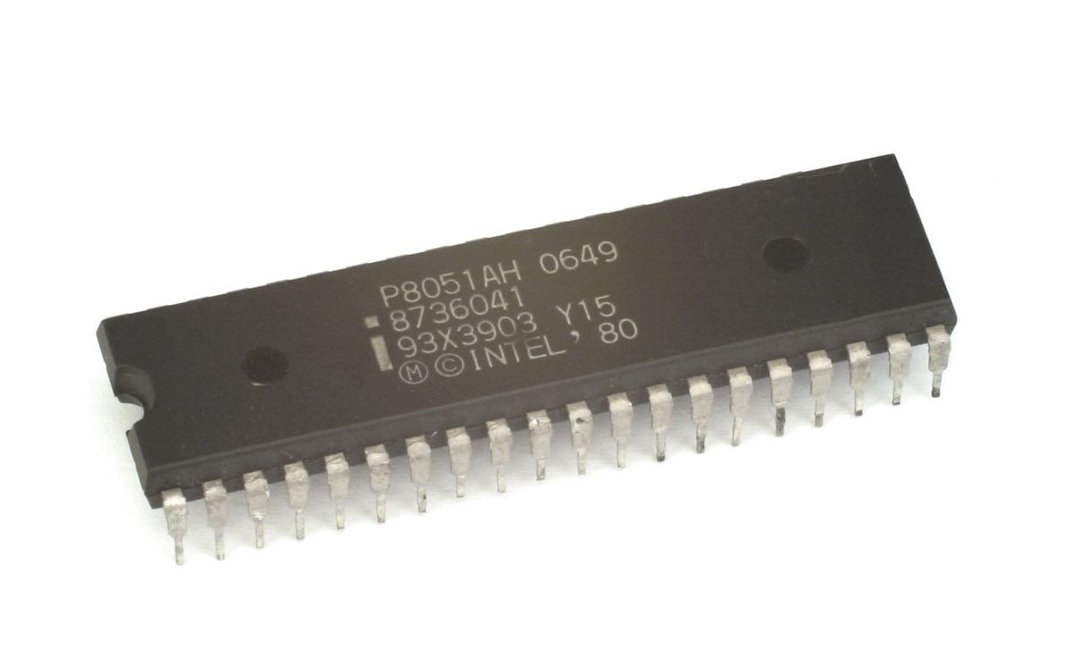
In 1981, Intel corporation introduced an [8-bit microcontroller] called the 8051 microcontroller.
- 4 kilobytes (4096 bytes) ROM on chip.
- 128 bytes on chip RAM.
- 32 bidirectional I/O lines organised as four 8-bit ports(P0, P1, P2 and P3)
- 4 kilobytes (4096 bytes) ROM on chip.
- 128 bytes on chip RAM.
- 32 bidirectional I/O lines organised as four 8-bit ports(P0, P1, P2 and P3).
- Two multiple mode, 16-bit Timer / counter.
- Multiple mode, high speed programmable serial port.
- Two-level interrupt structure.
- Four register banks of 8 registers each.
- 128 user defined software flags.
- 64 kilobytes of external memory access.
- 256 I/O devices can interface.
- Integrated Boolean processor for control application.
- Direct byte and bit addressability.
- Single + 5V power supply operation.
- NMOS technology.
- It is referred as “system on chip”.
It is an 8- bit processor, means processor (CPU) can work on only 8 bits of a data at a time. Data larger than 8 bit has to be broken into 8 pieces to be processed by the CPU.
- Binary or singed arithmetic.
- Signed overflow detection.
- Parity computation.
- Hardware multiple and divide in 4 microseconds.
- Available in DIP plastic packaging.
- It is a 40-pin IC.
Block diagram of 8051 microcontroller
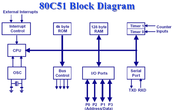
The above figure shows internal block diagram of 8051. It consists of Central Processing Unit (CPU), two kinds of memory (1) DATA RAM and (2) Programmable ROM / EPROM; Input/output ports, mode status and data registers. These elements communicate through an eight-bit data bus which runs through the chip referred as internal data bus.
| (MSB) | (LSB) | ||||||
|---|---|---|---|---|---|---|---|
CY |
AC |
F0 |
RS1 |
RS0 |
OV |
- | P |
| Symbol | Position | Function |
|---|---|---|
CY |
PSW.7 |
Carry Flag |
AC |
ACPSW.6 |
Auxiliary Carry Flag. For BCD Operations |
ACF0 |
ACPSW.5 |
Flag 0. Available to the user for general purposes |
ACRS1 |
ACPSW.4 |
Register bank select bits. Set by software to determine which registers are being used |
ACRS0 |
ACPSW.3 |
|
ACOV |
ACPSW.2 |
Overflow Flag |
| - | ACPSW.1 |
Not used |
ACP |
ACPSW.0 |
Partiy Flag. Even Parity |
Basic information bout the PSW register
- It is an 8-bit register.
- It is also referred as flag register.
- Only 6 bits of the PSW are used by 8051.
- Two unused bits are user definable flags.
- Four of the flags are called as conditional flags. They are
CY,P,ACandOV. - Two of the flags are used to select register bank.
CY (Carry Flag):
- This flag is set whenever there is carry out from of bit.
- This flag bit is affected after an 8-bit addition or subtraction.
- It can also be set to 1 or 0 directly by an instruction such as ‘
SETB’ (Set Bit Carry) and ‘CLR C’(Clear Carry).
AC (Auxiliary Flag):
- This flag is affected only after addition.
- If there is a carry from D3 to D4 bit during an addition, this bit is set otherwise this bit is reset.
- This flag is used by an instruction that performs BCD addition.
P (Parity Flag):
- This flag is affected by number of 1s in an accumulator register.
- If the A register containins an odd number of 1’s then this flag is set, otherwise if the number of 1’s in the A register is even then this bit is reset.
OV (Overflow Flag):
- This flag is set whenever the result of a signed number operation is too large, otherwise it is reset.
- If you want to divide any number by zero then the result is too large (infinite) at that time this flag is set, otherwise, it is reset.
RS1, RS0 (Register Selection Bank):
| RS1 | RS0 | Register Bank | Address |
|---|---|---|---|
| 0 | 0 | 0 | 00H-07H |
| 0 | 1 | 1 | 08H-0FH |
| 1 | 0 | 2 | 10H-17H |
| 1 | 1 | 3 | 18H-1FH |
The remaining two bits are general purpose status flag bits and can be used by the programmer for any purpose. In other words, they are user defined bits.
128 byte memory
- R0 to R127 (
00Hto7FH)
Divided into three sections
- Register Banks (32)
- R0 to R31 (
00Hto1FH) - Bit Addressable RAM (16)
- R32 to R47 (
20Hto2FH) - Scratch Pad RAM (80)
- R48 to R127 (
30Hto7FH)
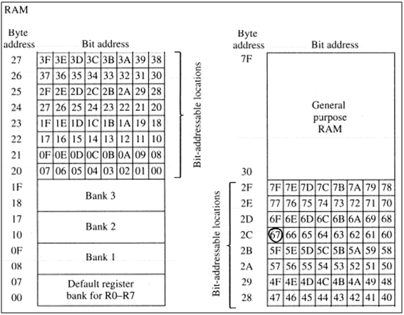
RAM Allocation
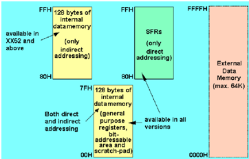
- There is 128 bytes of on chip RAM in 8051 plus number of special function register.
- These 128 bytes of RAM inside 8051 are assigned addresses
00Hto7FH. - Special function registers are assigned addresses from
80HtoFFH - 128-byte Data memory allocation is shown in the above figure
These 128 bytes are divided into three groups:
- A total of 32 bytes from locations
00Hto1FHare set aside for register banks and the stack. - 2A total of 16 bytes from locations
20Hto2FHare set aside for bit addressable read/write memory. - Remaining locations
30Hfrom to7FHare called as general-purpose RAM or scratch pad RAM.
Register bank in 8051 microcontrollers:
A total of 32 bytes of RAM are set aside for the register banks and stacks. These 32 bytes are divided into 4 banks of register in which each bank has 8-registers, R0 to R7. The above figure shows how the 32 bytes are allocated into 4 banks. From the above figure, bank 1 uses the same RAM space as the stack. This is a major problem in programming 8051. We must either not use register bank 1, or we must allocate another area of RAM for stack.
BIT addressable RAM
Out of the 128 bytes internal RAM of the 8051, 16 bytes of it are bit addressable.Each bit of sixteen bytes from 20H to 2FH has individual bit address.Bit address varies from 00H to 7FH as shown in the figure below.
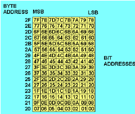
The rest must be accessed in byte format.The bit addressable RAM locations are 20H to 2FH.These 16 bytes provide 128 bits of RAM, addressed as 0 to 127 (in decimal) or 00H to 7FH in hexadecimal.The internal RAM locations 20 H to 2FH are both byte addressable and also bit addressable.
Scratch Pad RAM
30H-7FH is available to the user as data RAM. However, if the data pointer has been initialized to this area, enough bytes should be left aside to prevent SP data destruction.
Special Function Registers (SFR):
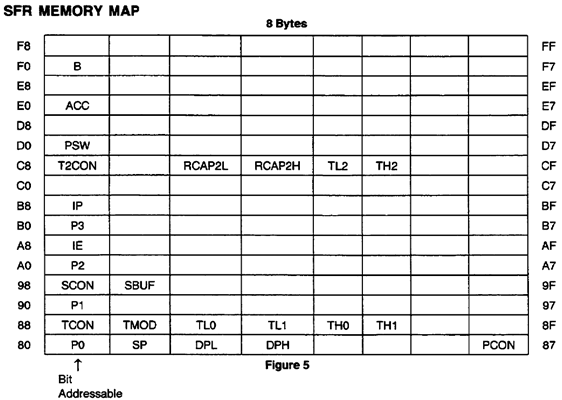
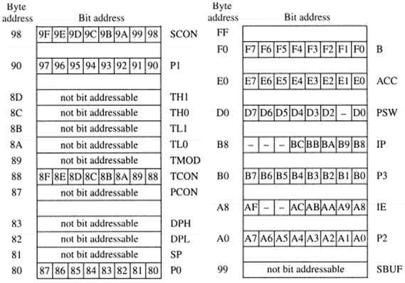
Unlike other microprocessor in the Intel Family, 8051 uses memory mapped I/O through a set of Special Function Registers (SFRS). SFR are of 128 bytes and that are implemented in the address space immediately above the 128 bytes of RAM. Fig. 1.14 shows SFR starts from 80 H and ends at FFH.SFR is a bit addressable area. All access to the four I/O ports, the CPU, interrupt control register, the timer / counter, UART and power control are performed through Special Function Registers (SFR) between 80H and FFH.
Input / Output Ports
- The 8051 each have 32 I/O pins configured as 4-eight-bit parallel ports. [P0, P1, P2 and P3].
- Each pin will be input or output or both under software control.
- After reset, 8051 writes logic 1 (Input) on every pins.
- Port 0 and Port 2 in combination can be used to interface external memory.
- Port-3 pins have special functions such as two external interrupt, two counter input, two special data lines, and two-timing control strobe.
Timer
- The 8051 has 16 bit timers that can be operated in four different modes.
- Timer can be configured using Timer/counter control/status register.
- These timers can also be used as counter that increments after each clock pulse applied to T0 and T1 pin.
Serial interface
- A full duplex asynchronous serial interface can be implemented on chip, using serial interface control circuitry.
- The special feature of this circuit is a double buffered receiver.
Interrupts
- The 8051 has five hardware interrupt sources, one from the serial port, when transmission or reception is completed, two from the timers when overflow occurs, and two from the interrupt pin INT0 and INT1.
- Each interrupt has its own vector location.
Input / Output Ports
- The 8051 each have 32 I/O pins configured as 4-eight-bit parallel ports. [P0, P1, P2 and P3].
- Each pin will be input or output or both under software control.
- After reset, 8051 writes logic 1 (Input) on every pins.
- Port 0 and Port 2 in combination can be used to interface external memory.
- Port-3 pins have special functions such as two external interrupt, two counter input, two special data lines, and two-timing control strobe.
Accumulator (A) and B registers
- Both of them are 8-bit registers.
- Accumulator holds the source operand and receives the result of arithmetic instructions.
- The accumulator can be source or destination for logical operations and number of special data movement instructions.
- Several functions apply only to an accumulator such as rotate, parity computation, testing for zero.
- B-register is an 8-bit register available for general purpose.
Stack Pointer (SP)
- It is an 8-bit register.
- It is incremented before data is stored during PUSH and CALL instructions.
- The stack array resides anywhere in on chip RAM.
- The SP register is initialised to
07Hafter a reset. - This causes the stack to begin at
08H.
Data Pointer Register (DPTR)
- It is a sixteen (16)-bit register.
- It consists of higher 8-bit (DPH) and lower 8-bit (DPL).
- It is function is to hold 16-bit address.
- It may be manipulated as a 16-bit data register or as two independent 8-bit register.
- It serves as base register in indirect jumps, lookup table instructions and external data transfer..